Design and Validation of a CCE Antenna for LoRa
Design of a 915MHz capacitively coupled element (CCE) antenna using the emerge python library for an upcoming LoRa flight computer
Henry Chen
11 April 2026
Introduction
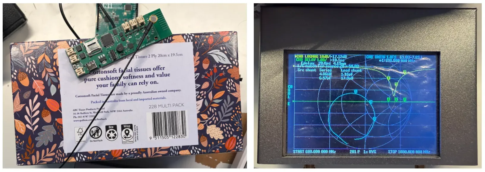
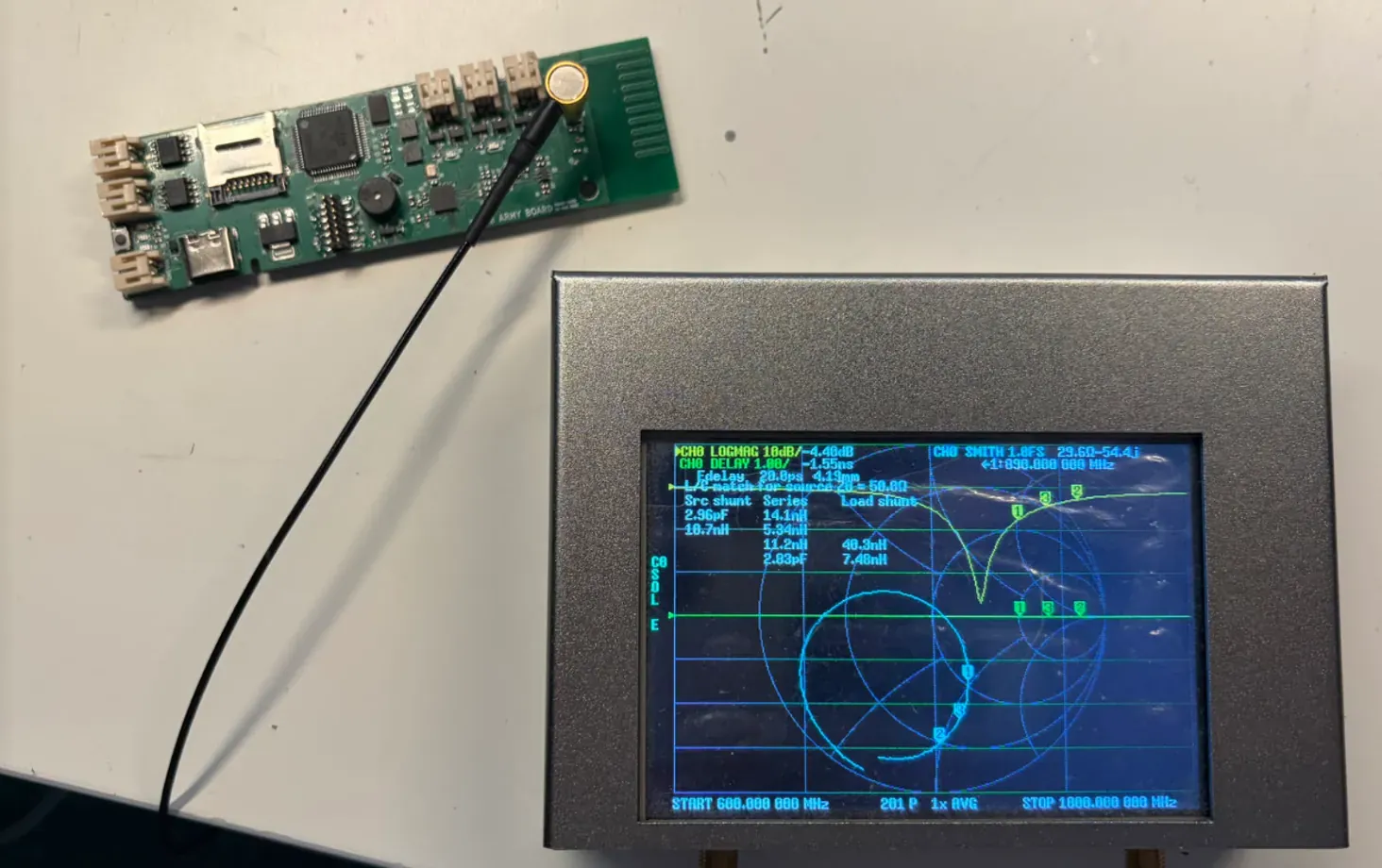
Recently, A resonant helical antenna was used on a recently designed flight computer to enable LoRa communication on the 915-928MHz Band. This was to enable remote launch and flight telemetry during flight at >5km line of sight. It turns out, the implementation of the antenna was rather fickle. It exhibited significant detuning sensitivity, very narrow bandwidth and poor resonance at 915MHz - opting to resonate at 890MHz instead. This made the design unsuitable for use in Australia. Furthermore, even at 890MHz, the boards were unable to transmit between each other during bringup - largely due to detuning. Capacitively coupled element (CCE) antennas promised to be a good alternative - especially for via-stitched 4-layer PCBs. This blog article demonstrates the use of a 6mm x 6mm square pad placed at the corner of the existing PCB. This element would cause the the ground plane to resonate by capacitive coupling it to the RF source. The antenna was designed using a finite element solver called emerge. It was then embodied as a physical prototype by etching out the antenna and tuning geometry on copper clad FR4. A matching network was then implemented using a NanoVNA. The prototype achieved an improved return loss of -26dB at 916MHz - a significant improvement over the original -20dB at 886 MHz. Furthermore, the antenna's succeptibility to detuning was reduced significantly - maintaining resonance at 916MHz even when touched.
Background and Theory (CCE Principles)
Modern devices demand antennas that are more compact, broadband and robust - a combination that self-resonant antennas such as PIFAs, Helical and dipole antennas struglgle to meet. A resonant antenna must be physically tuned to the target frequency which, at 915 MHz, implies at least a quater wavelength of approx. 82mm. Achieving this in a PCB form factor forces designers into compromises such as meandering traces, tight tolerances and easily detuned antennas. In these cases, any nearby dielectric can shift the resonant frequency of the antenna, narrow the bandwidth of the structure and ultimately degrade link performance.
The CCE antenna, first proposed by Vainikainen et al in the early 2000s addresses this problem by abandoning the notion of resonant elements. Instead, they opted to place small, geometrically simple conductive pads - non resonant by design - in the corner or short edge of the PCB ground plane and exploiting the wave mode of the device's chassis instead. When RF power is applied, the CCE capacitively couples energy int the ground plane, causing it to resonate and thus, radiate, as a half-wave dipole antenna. In future works, this was extended to cause the groudn plane to radiate in higher order wave modes as well. In these classes of antennas, the CCE is merely a coupler, and a separate lumped-element matching network is used to tune the resonant frequency. Because the antenna structure becomes the relatively large ground plane, it can support lower a lower radiation quality factor therefore, achieving a wider bandwidth for the same footprint size.
Furthermore, they are much more robust to detuning. This is because touching the ground plane has little effect as the radiation mode is distributed accross the entire surface. Touching the CCE element, however does effec the resonant point of the antenna as it adds capacitance to the load that is not compensated by the matching network. Due to the size of the elemnt, however, it remains largely robust even if the dieletric is spaced >3-5mm away. This is because the capacitive contribution of the dieletricl to the pad is significatnly reduced - helped also by the significantly reduced pad area. This translates to minimal constratins when it comes to housing design for the antenna - mandating only that a minor air gap be present around the CCE.
Methodology
Simulation Modelling
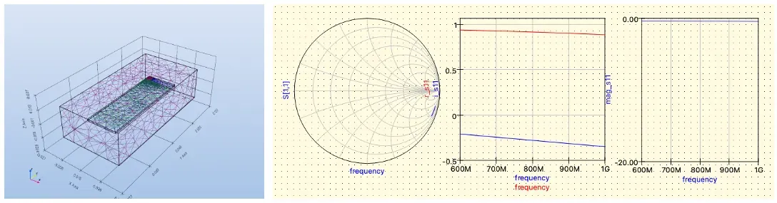
Simulations were run using this emerge script. The simulations proved promising however, it indicated tuning of a sufficient matching network was required.
Mesh Design
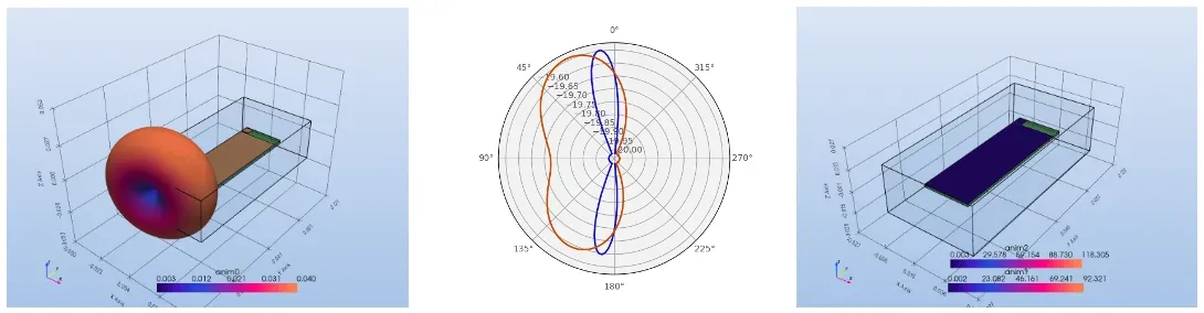
Far Field and Current Distribution
Physical Prototyping and Characterization
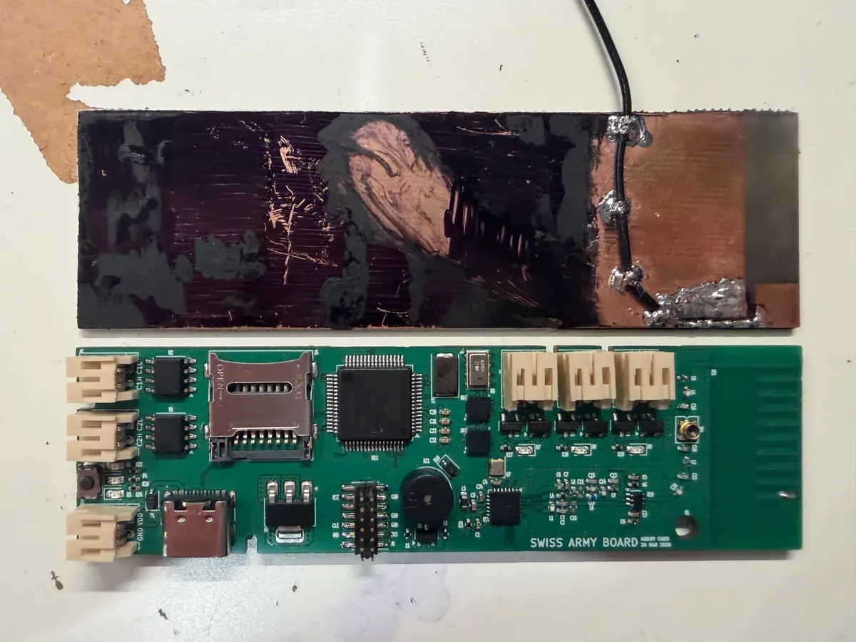
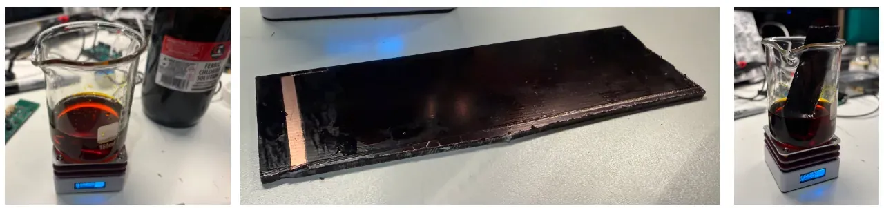
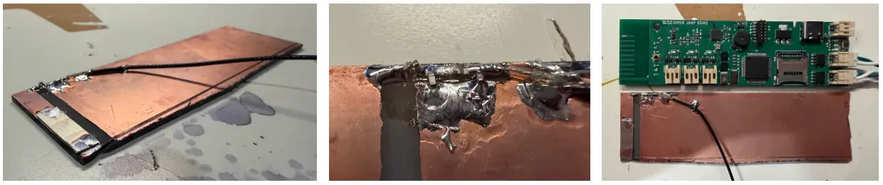
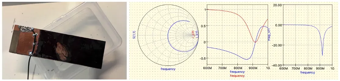
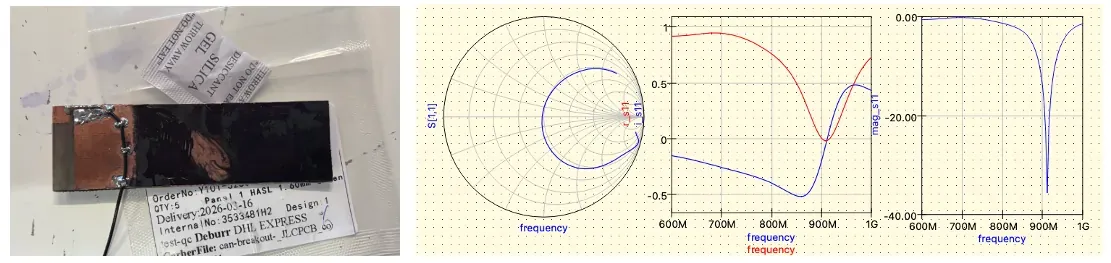
The prototype was built on copper clad FR4. A 100mm x 30mm board outline was scored into the fibreglass with a stanley knife and snapped to shape. The CCE geometry and matching network pads were then drawn onto the copper surface using a fine-tip permanent marker - acting as the etch resist.
The board was partially submerged and etched in 60 mL of 90°C 1:1 ferric chloride and water solution. At this temperature, etching completed in under five minutes. The solution was agitated throughout to further speed up the etching process and circulate the etchant. Care was taken not to over-etch, as fine features could have been lost. Uniform application of the etch resist was found to be critical — thin or patchy coverage resulted in uneven etching and over-etched patches throughout the submerged part of the board.
Impedance Matching
-
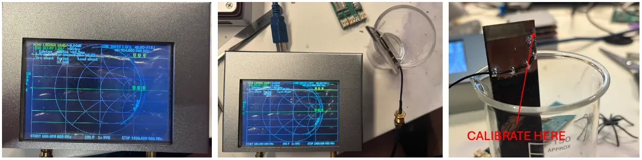
Load, Short and Open Calibration applied at antenna feed point.
-
Following suggested passives on the NanoVNA;
-
final match was series 39nH with 3pF series following; apologises for not having a 36nH inductor.
Results and Discussion
Compare performance and argue why the CCE solution is better
Original Antenna Performance
Comparative Analysis
| Configuration | Center Freq | Min Freq | Max Freq | Max Return Loss |
|---|---|---|---|---|
| Unmatched | 910 MHz | 826 MHz | 962 MHz | -4.43 dB |
| Matched Ontop of Box | 862 MHz | 810 MHz | 932 MHz | -19.93 dB |
| Matched On Edge of Box | 884 MHz | 832 Mhz | 952 MHz | -20.37 MHz |
| Matched on Table Top | 846 MHz | 770 MHz | 918 MHz | -22.46 dB |
Prototype Antenna Performance
| Configuration | Center Freq | Min Freq | Max Freq | Max Return Loss |
|---|---|---|---|---|
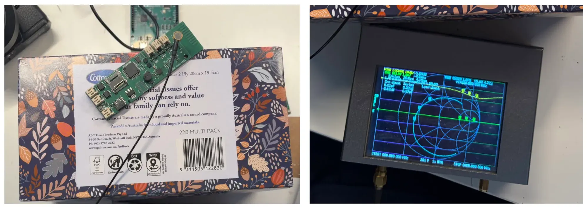
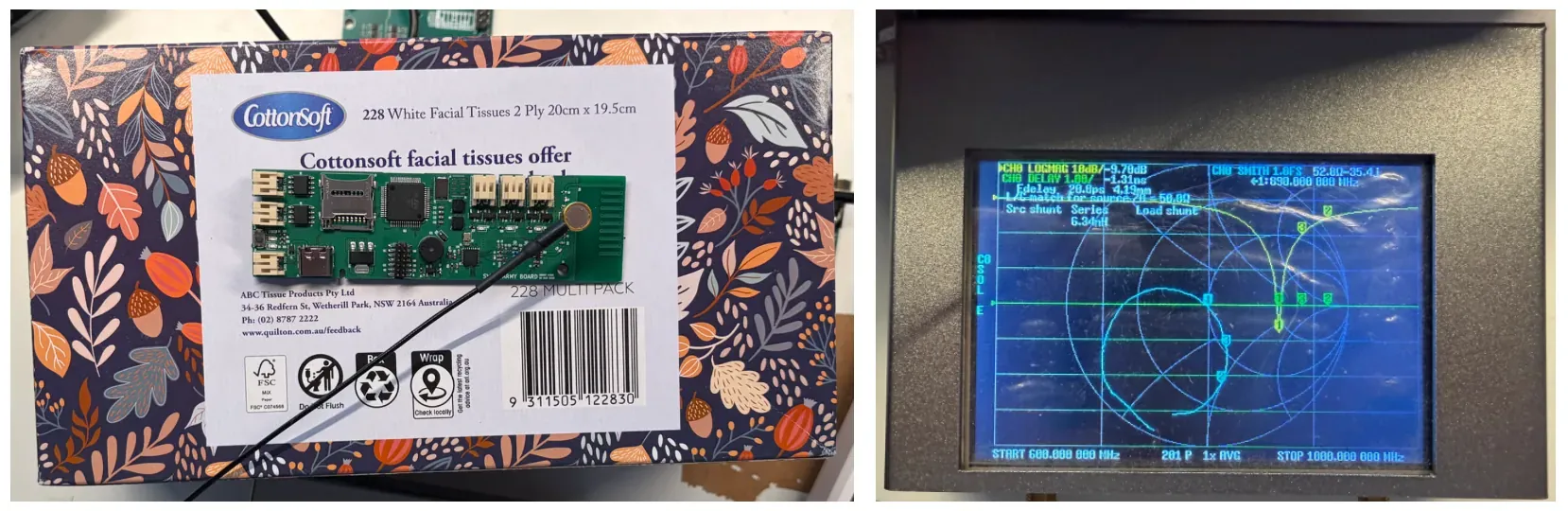
| Baseline | 916 MHz | 868 MHz | 972 MHz | -26 dB |
| Touching GND Plane | 916 MHz | 868 MHz | 968 MHz | -21 dB |
| Touching Table | 868 MHz | 812 Mhz | 936 MHz | -32 MHz |
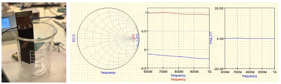
| 3-5mm Elevated | 912 MHz | 852 Mhz | 968 MHz | -35.65 dB |
| 1.5cm Elevation | 920 MHz | 872 MHz | 968 MHz | -23.7 dB |
Although not captured here, the CCE antenna is extremely sensitive to materials beneath and above. A 3mm airgap is likely required. This extends to the housing design. This may be remedied by creating a 3mm high CCE chip antenna instead however, this is not explored here.
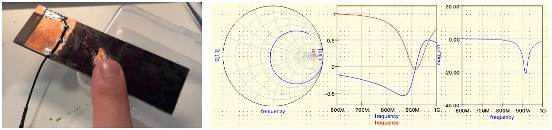
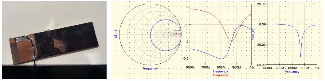
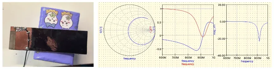
The antenna is tolerant of touching on the opposite long-side of the antenna (where the current distribution is not present). It is also tolerant of touching on the middle part of the same long-side as the antenna. it is affected when you touch the null at the bottom of the board on the same long side as the antenna;
- performance is much more robust. has more than sufficient return loss at 915MHz; compared to the original 890MHz of the original antenna;
- antenna is more robust to touch than the origional antenna as indicated by the reduced shift in center frequency;
- antenna is more robust to mounting materials compared to original antenna;
- leads to more flexible mounting arrangements in practice;
Present initial unoptimized CCE data (Baselien and Simulated)
- antenna is inheriently capacitive as explained in theory;
- this matches the simulated return loss shown above; starting point is similar although with expected discrepancies due to measurement error.
Impact of Environment and Coupling
- Resonance Tuning: how was the matching network built
- Environmentlal Sensitivitty: explain the performance changes to the backing material are applied.
- Illustrate the need for the 3mm airgap underneath the CCE;
- Explain how the capacitance to the surrounding environment chances performance
- conclude antenna performance is highly dependant on the coupling environment and to make sure you control spacing around the antenna during deployment
- note the performance other antenna strucutres; larger capacitance when the CCE was wider made it much ahrder to tune
Practical Considerations and Future Work
- Implications for Production
- cost savings for board; more robust performance and space savings mean you get more space for components; leads to single sided assembly for the design
- etching and prototypig the board required a fine tip permannt market to achieve good accuracy and definition for antenna geomoetries;
- during prototyping, maek sure you heat the etchant to 90C for best performance. swirl the etchat as well to circulate if you dont have a stirring element
- Further Development
- housing needs to be carefuly designed to maintain clearance epsecially around the CCE antenna
- integration onto real-world respin of the board is imminent
- integrate the CCE onto a custom 1.6mm chip antenna instead to elevate it 3mm above ground when mounted onto the board? makes the board more suited for using on the table
Conclusion
- recap: to achieve 5km with LoRa, its imperative a robust antenna is used.
- method summary: simulated, etched, tuned and measured the performance of a custom CCE antenna before respinning the board
- The CCE provides superior and more robust return loss compared to its resonant helical antenna counterpart at fraction of the board volume and footprint.
- confidence in shipping the board for manufacture